- 您现在的位置:买卖IC网 > Sheet目录341 > MAX5078BATT+T (Maxim Integrated Products)IC MOSFET DRIVER 6-TDFN
�� �
�
�MAX5078�
�4A,� 20ns,� MOSFET� Driver�
�Table� 1.� MAX5078� Truth� Table�
�IN+�
�Low�
�Low�
�IN-�
�Low�
�High�
�OUT�
�Low�
�Low�
�V� DD�
�MAX5078�
�High�
�Low�
�High�
�PWM�
�INPUT�
�IN+�
�OUT�
�High�
�High�
�Low�
�Use� the� following� PC� board� layout� guidelines� when�
�designing� with� the� MAX5078A/MAX5078B:�
�ON�
�OFF�
�IN-�
�GND�
�?�
�Place� one� or� more� 0.1μF� decoupling� ceramic�
�capacitors� from� V� DD� to� GND� as� close� to� the� device�
�as� possible.� Connect� V� DD� and� GND� to� large� copper�
�areas.� Place� one� bulk� capacitor� of� 10μF� (min)� on�
�the� PC� board� with� a� low� resistance� path� to� the� V� DD�
�input� and� GND� of� the� MAX5078A/MAX5078B.�
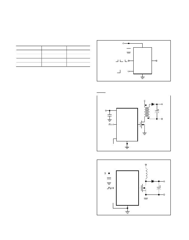
�Figure� 3.� Unused� Input� as� an� ON/OFF� Function�
�Additional� Application� Circuits�
�?�
�Two� AC� current� loops� form� between� the� device� and�
�the� gate� of� the� driven� MOSFET.� The� MOSFET� looks�
�V� S�
�like� a� large� capacitance� from� gate� to� source� when� the�
�gate� pulls� low.� The� active� current� loop� is� from� the�
�MOSFET� gate� to� OUT� of� the� MAX5078A/MAX5078B,�
�V� DD�
�V� DD�
�to� GND� of� the� MAX5078A/MAX5078B,� and� to� the�
�source� of� the� MOSFET.� When� the� gate� of� the� MOSFET�
�pulls� high,� the� active� current� is� from� the� V� DD� terminal�
�of� the� decoupling� capacitor,� to� V� DD� of� the�
�IN+�
�MAX5078A�
�MAX5078B�
�OUT�
�N�
�MAX5078A/MAX5078B,� to� OUT� of� the� MAX5078A/�
�MAX5078B,� to� the� MOSFET� gate,� to� the� MOSFET�
�source,� and� to� the� negative� terminal� of� the� decoupling�
�capacitor.� Both� charging� current� and� discharging�
�current� loops� are� important.� Minimize� the� physical� dis-�
�tance� and� the� impedance� in� these� AC� current� paths.�
�IN-�
�GND�
�?�
�?�
�?�
�Keep� the� device� as� close� to� the� MOSFET� as� possible.�
�In� a� multilayer� PC� board,� the� inner� layers� should�
�consist� of� a� GND� plane� containing� the� discharging�
�and� charging� current� loops.�
�Pay� extra� attention� to� the� ground� loop� and� use� a�
�low-impedance� source� when� using� a� TTL� logic-�
�input� device.� Fast� fall� time� at� OUT� may� corrupt� the�
�Figure� 4.� Noninverting� Application�
�4V� TO� 15V�
�V� DD�
�V� S�
�input� during� transition.�
�Exposed� Pad�
�MAX5078A�
�V� OUT�
�The� TDFN-EP� package� has� an� exposed� pad� on� the� bot-�
�MAX5078B�
�tom� of� its� package.� This� pad� is� internally� connected� to�
�GND.� For� the� best� thermal� conductivity,� solder� the�
�exposed� pad� to� the� ground� plane� in� order� to� dissipate�
�FROM� PWM�
�CONTROLLER�
�(BOOST)�
�IN+�
�OUT�
�N�
�1.9W.� Do� not� use� the� ground-connected� pad� as� the�
�only� electrical� ground� connection� or� ground� return.� Use�
�GND� (pins� 2� and� 3)� as� the� primary� electrical� ground�
�IN-�
�GND�
�connection.�
�Figure� 5.� Boost� Converter�
�10�
�Maxim� Integrated�
�发布紧急采购,3分钟左右您将得到回复。
相关PDF资料
MAX5092EVKIT+
KIT EVALUATION FOR MAX5092
MAX620EWN
IC DVR QUAD HISIDE MOSFET 18SOIC
MAX626CPA+
IC DRIVER MOSFET DUAL 8-DIP
MAX662EVKIT-SO
EVAL KIT FOR MAX662
MAX6947ATE+T
IC LED DRIVER LINEAR 16-TQFN
MAX6948BGWA+T
IC LED DVR PWM GPIO 25WLP
MAX6964ATG+T
IC LED DRIVER LINEAR 24-TQFN
MAX6965ATE+T
IC LED DRIVER LINEAR 16-TQFN
相关代理商/技术参数
MAX5078BATT-T
功能描述:功率驱动器IC 4A 20ns MOSFET Driver RoHS:否 制造商:Micrel 产品:MOSFET Gate Drivers 类型:Low Cost High or Low Side MOSFET Driver 上升时间: 下降时间: 电源电压-最大:30 V 电源电压-最小:2.75 V 电源电流: 最大功率耗散: 最大工作温度:+ 85 C 安装风格:SMD/SMT 封装 / 箱体:SOIC-8 封装:Tube
MAX5079
制造商:MAXIM 制造商全称:Maxim Integrated Products 功能描述:ORing MOSFET Controller with Ultra-Fast 200ns Turn-Off
MAX5079_09
制造商:MAXIM 制造商全称:Maxim Integrated Products 功能描述:ORing MOSFET Controller with Ultra-Fast 200ns Turn-Off
MAX5079EUD
功能描述:功率驱动器IC RoHS:否 制造商:Micrel 产品:MOSFET Gate Drivers 类型:Low Cost High or Low Side MOSFET Driver 上升时间: 下降时间: 电源电压-最大:30 V 电源电压-最小:2.75 V 电源电流: 最大功率耗散: 最大工作温度:+ 85 C 安装风格:SMD/SMT 封装 / 箱体:SOIC-8 封装:Tube
MAX5079EUD+
功能描述:功率驱动器IC ORing MOSFET Controller RoHS:否 制造商:Micrel 产品:MOSFET Gate Drivers 类型:Low Cost High or Low Side MOSFET Driver 上升时间: 下降时间: 电源电压-最大:30 V 电源电压-最小:2.75 V 电源电流: 最大功率耗散: 最大工作温度:+ 85 C 安装风格:SMD/SMT 封装 / 箱体:SOIC-8 封装:Tube
MAX5079EUD+T
功能描述:功率驱动器IC ORing MOSFET Controller RoHS:否 制造商:Micrel 产品:MOSFET Gate Drivers 类型:Low Cost High or Low Side MOSFET Driver 上升时间: 下降时间: 电源电压-最大:30 V 电源电压-最小:2.75 V 电源电流: 最大功率耗散: 最大工作温度:+ 85 C 安装风格:SMD/SMT 封装 / 箱体:SOIC-8 封装:Tube
MAX5079EUD+TG48
制造商:Maxim Integrated Products 功能描述:ORING MOSFET CONTROLLER WITH ULTRA-FAST 200NS TURN-OFF - Tape and Reel
MAX5079EUD-T
功能描述:功率驱动器IC RoHS:否 制造商:Micrel 产品:MOSFET Gate Drivers 类型:Low Cost High or Low Side MOSFET Driver 上升时间: 下降时间: 电源电压-最大:30 V 电源电压-最小:2.75 V 电源电流: 最大功率耗散: 最大工作温度:+ 85 C 安装风格:SMD/SMT 封装 / 箱体:SOIC-8 封装:Tube